❖ A snubber circuit consists of a series combination of resistance Rs and capacitance Cs in parallel with the thyristor.
❖ Strictly speaking, a capacitor C, in parallel with the device is sufficient to prevent unwanted dv/dt triggering of the SCR.
❖ When switch S is closed, a sudden voltage appears across the circuit. Capacitor Cs behaves like a short circuit, therefore voltage across SCR is zero.
❖ With the passage of time, voltage across Cs builds up at a slow rate such that dv/dt across Cs and therefore across SCR is less than the specified maximum dv/dt rating of the device.
❖ Here the question arises that if Cs is enough to prevent accidental turn-on of the device by dv/dt, what is the need of putting Rs in series with Cs ?
The answer to this is as given below
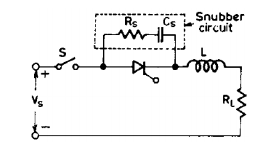
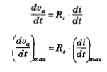
❖ Soon after the instant of closing the switch S is as shown in Fig., the voltage equation is
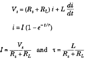
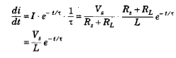
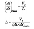
The value of di/dt is maximum when t=0
The voltage across SCR is given by, va=Rs.i
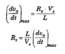
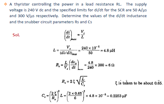
❖ Consisting of R, L, C should be fully analyzed to determine the optimum values of snubber circuit parameters Rs, Cs.
❖ The analysis of this circuit shows that resistance Rs can be obtained from the relation.
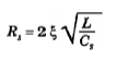
❖ Where ξ is the damping factor (damping ratio), In order to limit the peak voltage overshoot across thyristor to a safe value, damping factor in the range of 0.5 to 1 is usually used.
❖ For optimum solution of the problem, ξ is taken to be about 0.65
Password: Snubber
pdf made by Dr M Balasubbareddy